This section contains the user guides for the following tools: Block JIG Generator, Compare GDSII, Gerber to PCB,
Make Board Paneling, Metal Mask Manager, Mounting Data Extractor, Mounting Emulator, Router-Machine JIG Generator,
Solder Quantity Calculator, Soldering Pallet, Test Point Location Generator, and Underfill.
Block JIG Generator is used for the purpose of stable supporting the bare PCB and evenly applying lead in the screen printer equipment
that prints the solder cream during the SMD process.
Use Make Board Paneling to modify the data designed with a single sub board into an array type to use manufacturing
related features, such as Metal Mask Manager, Mounting Emulator, Block JIG Generator, and Router-Machine JIG Generator.
Metal Mask Manager is a tool that can register standard metal mask database, manage metal mask changing history, and check differences
between design and standard metal mask.
The PollEx Mounting Data Extractor function extracts components and PCB information for chip mounter from PCB design data. It is included in the PollEx PCB Modeler.
The Solder Quantity Calculator provides evidence to get numerical calculation and solder quantity based on whole mask space and user-defined
conditions.
This section contains the user guides for the following tools: BOM, CAM, Component Arrangement Plan, CP, Golden Sample,
Logic, PCB, Redmark+, and Worksheet Planner.
This section contains the user guides for the following tools: Block JIG Generator, Compare GDSII, Gerber to PCB,
Make Board Paneling, Metal Mask Manager, Mounting Data Extractor, Mounting Emulator, Router-Machine JIG Generator,
Solder Quantity Calculator, Soldering Pallet, Test Point Location Generator, and Underfill.
The Solder Quantity Calculator provides evidence to get numerical calculation and solder quantity based on whole mask space and user-defined
conditions.
Calculate solder quantity for reflow soldering process.
From the menu bar, click Manufacture > Solder Quantity Calculator > Metal Mask.
The User Metal Mask dialog opens. You can see pad
and metal mask on design.
U-Name List: View component and pin pads.
Metal mask size: View metal mask size for the selected pin.
Pad Size: View pad size for the selected pin.
Mask/Pad Ratio (%): View metal mask size ration related to pad size for the
selected pin.
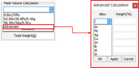
Mask Volume Calculation: After setting solder paste material, metal mask
thickness and correction factor (A/F: Aspect Ratio), click
Calculate to calculate total solder paste
weight.
Material: Metal Mask Manager supports three types of compound material
libraries.
Add a new material list by materials and composing ratio. Select
Advanced to complete making a new compound
material. Figure 1.
Default solder-paste materials’ unit weight depending on
compounding materials:
63Sn/37Pb: 0.0053
62.8Sn/36.8Pb/0.4Ag: 0.0053
96.5Sn/3Ag/0.5Cu: 0.0051
Mask Thickness: To calculate metal mask volume, specify the thickness
of the metal mask.
A /F Ratio (%): Use A/F ratio value to correct the area of metal
mask.
Total Weight (g): Use the equation Total Mask Volume * Solder Paste
Composing Material’s Weight.
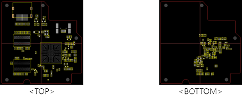
Choose View Setting Options.
Top/Bottom: Components that have a metal mask display. Figure 2.
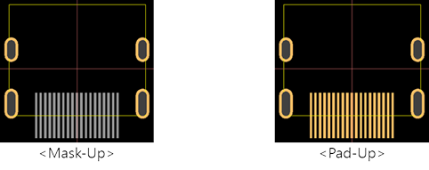
Mask-Top/Pad-Top: In most cases, pad size is bigger than metal mask
size, therefore Mask-Top view is preferred. Figure 3.
Zoom In/Zoom Out/Reset/Print: Same as PollEx PCB.
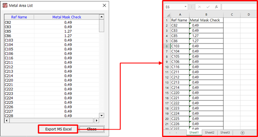
Display Metal Mask Area List: Check all the component’s metal mask sizes and
export the lists to the MS/Excel sheet. Make sure that the viewing list is not
mask-volume considering mask thickness, but dimension.