The Layer Stack menu shows PCB’s physical stacked information will be used for Signal
Integrity analysis.
From the menu bar, click Properties > Layer Stack. The Layer Stack dialog opens.
The stacking order, thicknesses and material
properties of metallic and dielectric layers are core parameters drawing dramatic
changes of signal transmission qualities and thermal distribution over PCB systems.
Therefore, precise assignment should be given to Type, Thickness,
Conductor/Dielectric Material, and the total thickness should be checked whether it
shows proper value. Other parameters can be
defined by clicking and
selecting one of the drop-down values. Layer Type for power plane should be defined
as Power and ground plane as Ground as displayed above. Available layer types are
coating, dielectric, signal, micro signal, power, ground, and floating layers. Each
layer type is described below:
Coating: Conformal coating material applied to protect the top and bottom
signal layers
Dielectric: Dielectric layer between two conductor layers. Multiple
dielectric layers can be placed next to each other
Signal: Etched signal layer. Core signal layer when microvias are used.
Micro Signal: For boards using microvias. Micro signal layers are made on
both sides of board.
Microvias are used for connecting micro signal layers or connecting a micro
signal layer and the first core layer.
Power: Power plane layer
Ground: Ground plane layer
Floating: Floating conductor plane layer
Often the top and bottom widths of etched conductor trace cross-section are
different, resulting in a trapezoidal cross-section shape.
PCB trace etching effect can be defined. The value of etching difference can be
typed in after double-clicking and the etching surface direction can be defined by
clicking .
PollEx PCB provides default layer stack set and user can add
or edit layer stack by clicking Import or
Export. The default layer stack file path is:
Installed directory/V6/Data/Layer. You can add, remove, or
insert each layer by clicking Add,
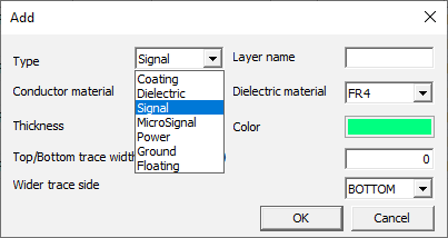
Remove, or Insert. By selecting
this menu, the Add dialog opens wherein you can set material
characteristics. You can export stack-up information as an Excel file. Figure 1.
 and
selecting one of the drop-down values. Layer Type for power plane should be defined
as Power and ground plane as Ground as displayed above. Available layer types are
coating, dielectric, signal, micro signal, power, ground, and floating layers. Each
layer type is described below:
and
selecting one of the drop-down values. Layer Type for power plane should be defined
as Power and ground plane as Ground as displayed above. Available layer types are
coating, dielectric, signal, micro signal, power, ground, and floating layers. Each
layer type is described below: