Gerber to PCB is a PCB generator from Gerber or ODB++ file,
which is non-intelligent data.
By importing a Gerber of ODB++ file, you can generate intelligent PCB design file
through the Gerber to PCB process.
ODB++
The ODB++ converts a limited ODB++ design file that has only graphical data into
PCB.
After converting to the intelligent PCB design, it can be used for the Bare Board
Test (BBT), which checks electrical liabilities on the PCB.
Launch PollEx PCB.
From the menu bar, click File > Open and open the PollEx_MFG_Sample_T3_r1.0.pdbb
file from
C:\ProgramData\altair\PollEx\<version>\Examples\MFG.
From the menu bar, click Manufacture > Gerber to PCB > ODB++.
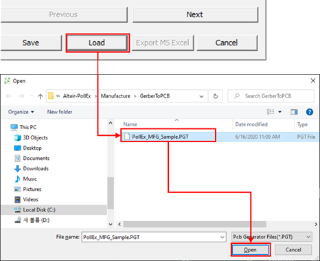
Click Load and select the
PollEx_MFG_Sample.pgt file from
C:\ProgramData\altair\PollEx\<version>\Examples\MFG\GerberToPCB.
Click Open.
Figure 1.
Click Next.
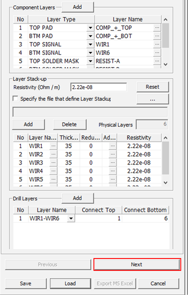
The pre-defined PCB Generator Files sets the Component Layers and Drill
Layers. Figure 2.
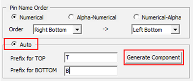
Make component.
Select Auto.
For Prefix for TOP, enter T.
For Prefix for BOTTOM, enter B.
Click Generate Component.
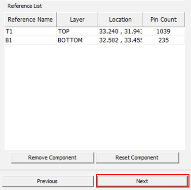
The components are automatically generated. Figure 3.
The generated lists for the TOP and BOTTOM are displayed in the
Reference List.
Click Next.
Figure 4.
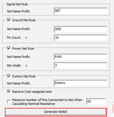
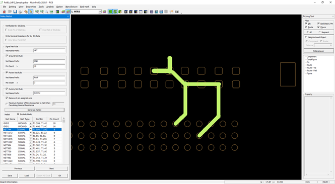
Make Netlist.
Under Signal Net Rule, enter NET for Net Name
Prefix.
Under Ground Net Rule, enter GND for Net Name
Prefix.
Under Power Net Rule, enter PWR for Net Name
Prefix.
Under Dummy Net Rule, enter Dummy for Net Name
Prefix.
Enable the Remove 0 pin assigned nets
checkbox.
Disable the Maximum Number of Pins Connected to Net When
Calculating Nominal Resistance checkbox.
Click Generate Netlist.
Figure 5.
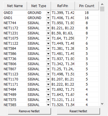
The created Netlists are displayed in the table. Figure 6.
Click NET744.
The selected net is highlighted in the design. Figure 7.
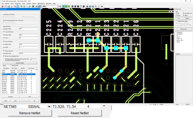
Enable the Exclude Mode checkbox.
Only the selected net is displayed. Figure 8.
Click Next.
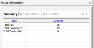
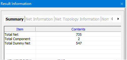
Review result information.
The result is displayed in each category such as: Summary, Net Information,
Net Topology Information, and Nominal Resistance. Figure 9.
In each tab, click a Net Name.
The selected net is displayed in the design.
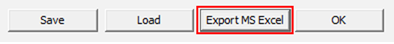
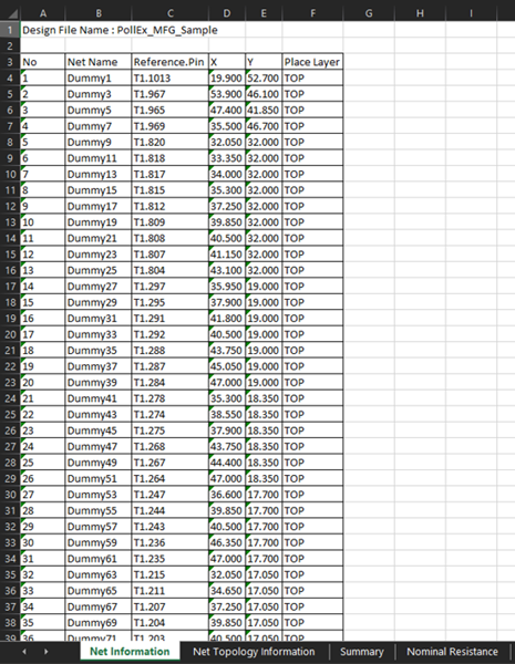
Export the result.
The result can be exported to Excel format.
Click Export MS Excel.
Figure 10. Figure 11.
Gerber + IPC-D-356
Gerber + IPC-D-356 converts a Gerber design file that has only graphical data into
PCB utilizing the IPC-D-356 data by reverse engineering.
Launch PollEx PCB.
From the menu bar, click File > Import ECAD > Gerber(RS-274D/RS-274X).
The Import from Gerber(RS-274D/RS-274X) dialog
opens.
In the Import from Gerber(RS-274D/RS-274X) dialog, click
.
Open all Gerber files from
C:\ProgramData\altair\PollEx\<version>\Examples\MFG\GerberToPCB\Gerber+IPC-D-356\gerber.
Click Import.
From the menu bar, click Manufacture > Gerber to PCB > Gerber + IPC-D-356.
Define layer setting.
There are two ways to set the layers, manually or by loading a predefined
environment file.
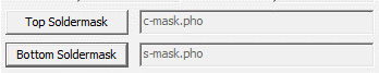
For Top Soldermask, select c-mask.pho.
For Bottom Soldermask, select s-mask.pho.
Figure 12.
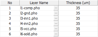
Define Layer Stack-up.
Click Add six times.
For 1, select l1-comp.pho for Layer Name.
For 2, select l2-gnd.pho for Layer Name.
For 3, select l3-inn1.pho for Layer Name.
For 4, select l4-inn2.pho for Layer Name.
For 5, select l5-vcc.pho for Layer Name.
For 6, select l6-sold.pho for Layer Name.
Figure 13.
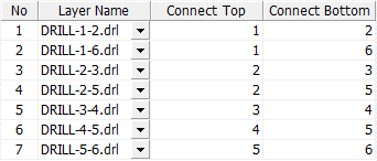
Define Drill Layers.
Click Add seven times.
Select layer names and enter the Connect Top and Connect Bottom values
as shown in Figure 14.
Figure 14.
Load Environment file.
If the environment file is loaded, steps 7 - 9 are not
required.
In the Layer Setting dialog, click
Load.
Select the Gerber_Env.DPCE file from
C:\ProgramData\altair\PollEx\<version>\Examples\MFG\GerberToPCB\Gerber+IPC-D-356.
Load IPC data.
Click and select the
IPC-D-356A.ipc file from
C:\ProgramData\altair\PollEx\<version>\Examples\MFG\GerberToPCB\Gerber+IPC-D-356\IPC-D-356A.
Click Generate Component.
Both the Gerber and IPC data are displayed as shown in
. Figure 15.
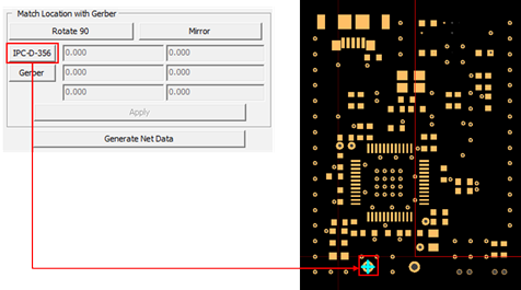
Match the Location of Gerber and IPC data.
Click IPC-D-356.
Click the component in the IPC data.
Figure 16.
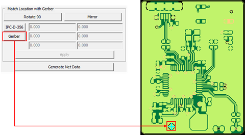
Click Gerber.
Click the component in the Gerber data.
Figure 17.
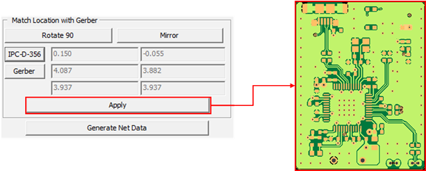
Selected coordinates are automatically entered in the
table.
Click Apply.
The data will be matched by moving the IPC data to the Gerber data
based on the selected component on each design. Figure 18.
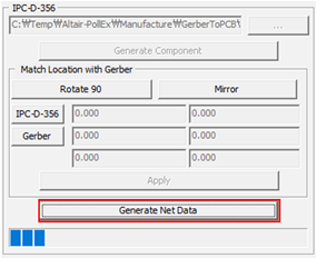
Click Generate Net Data.
Figure 19.
Review result.
Once the PCB design generation is completed, you can review the results of the
Summary, Net Information, and Net Error Data. In each tab, a selected net from
the lists will be focused and highlighted on the right-side of window for your
review. Figure 20.
 .
.