Verify that fiducial marks are designed correctly on the paneling board.
Define fiducial marks in the design with these methods:
Components registered with a fiducial mark.
Geometry drawing containing a fiducial mark.
A via being used as a fiducial mark.
The Fiducial Mark dialog contains the following
sections:
Fiducial Mark Definition
Component Group Selection: Select the fiducial-mark from the
predefined component group list. Use if the fiducial marks are
designed with components.
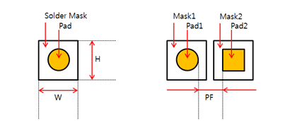
Mask1(S/R) Size (SS): Set the fiducial mark with the outer
mask size.
PAD1 Size (PS): Set the fiducial mark with the inner pad
size.
Mask2(S/R) Size (SS): Set the fiducial mark with the outer
mask size.
PAD2 Size (SS): Set the fiducial mark with the inner pad
size.
Recognize conductive figure shape as Pad: Recognize an
object as a pad. Use if the object is drawn with the figure
shape in the conductive layer.
Via: Select the fiducial mark from a via list used in active design.
Use if fiducial marks are designed with vias.
Board Figure Geometries: Set the size of the target objects. Use if
the fiducial mark is defined with a solder-mask and/or pad.
Mask1(S/R) Size (SS): Set the fiducial mark with the outer
mask size.
PAD1 Size (PS): Set the fiducial mark with the inner pad
size.
Mask2(S/R) Size (SS): Set the fiducial mark with the outer
mask size.
PAD2 Size (SS): Set the fiducial mark with the inner pad
size.
Mask/PAD Distance (PF): Set the fiducial mark with the
distance between the pads. Figure 1.
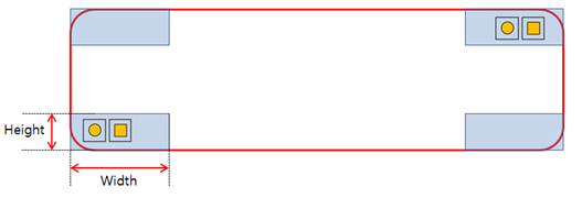
Fiducial Mark Searching Ranges from Board Corner & Layer: Set
the area where the fiducial mark is located from the board corner.
Use PollEx DFM to search the given area to
find the fiducial mark.
Searching Ranges: Set the width and height of the fiducial
mark search ranges starting from the specified board
corner. Figure 2.
Searching Layer: Set the layer where the fiducial mark is
located.
Fiducial Mark Placement Checking: Set the layer where the fiducial mark is
located.
Placement Layer Checking: Set the layer where the fiducial mark is
located.
Same On Specified Component: Set the fiducial mark location
as the same layer as a specified component. Use if all
components are placed on the top or bottom layer,
Bottom: Set the fiducial mark location as the bottom
layer.
Top: Set the fiducial mark location as the top layer.
Specifying Component: Set the component group that is used as the
fiducial mark.
Exceptional Component: Set the exceptional component group.
Not recognize as Fiducial Mark in Region out of Board Outline:
Exclude components as the fiducial mark if located outside of the
board outline.
Ignore the Fails for Marks placed on reverse Side: The analysis
passes when the fiducial marks are located on the reverse board
side. If the fiducial mark is located on the top and bottom layer
with the Top option checked, the bottom placed fiducial-mark fails
during analysis. With this option checked, the bottom placed
fiducial mark will pass.
Clearance Checking: Check various clearances with the fiducial mark.
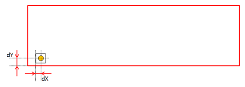
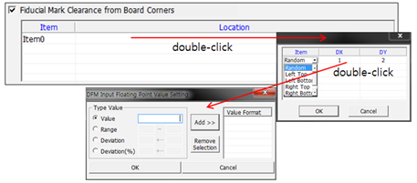
Fiducial Mark Clearance from Board Corners: Verify that the fiducial
marks are placed in the proper position. Define a suitable area for
placement from the board edge corners. Figure 3.
Set the fiducial mark clearance value from each of the board
outline corners using the Floating Value Range Input tool. Figure 4.
Clearance between Fiducial Mark and Via: Verify the clearance
between a via and the fiducial mark.
Clearance between Fiducial Mark and Routing Patterns: Verify the
clearance between route patterns and the fiducial mark.
Clearance between Fiducial Mark and Components: Verify the clearance
between components and the fiducial mark.
Other Checking
Diagonal Existence: Verify that the fiducial-marks are placed
diagonally. If there is no diagonal placement, the analysis
fails.
Number of Mark in Diagonal Corner: Define the number of fiducial
marks in each corner. If the number of marks does not match with the
given number, the analysis fails.
Minimum Number of Marks in each Layer: Verify the number of
fiducial-marks placed on each corner of the board. Use the minimum,
minimum or equal, or equal option for the given integer value.
Overlapping with Copper-Pour: Verify that copper is located in the
fiducial mark region. The two cannot be placed on the same
region.
Overlapping with Silkscreen: Verify there is overlapping with
objects on the top and/or bottom silkscreen layers.
Top: Select the GERBER silkscreen top layer from the artwork
layer list.
Bottom: Select the GERBER silkscreen bottom layer from the
artwork layer list.
Alignment (X, Y) of Mark: Verify the alignment of the fiducial mark.
The fiducial mark coordination values of X or Y must be the same if
it is not placed diagonally.
Overlapping with Holes: Verify the fiducial marks are overlapped
with the mechanical hole.
Symmetry Placement: Verify the fiducial marks are placed
symmetrically.
Non Symmetry Placement: Verify the fiducial-marks are not placed
symmetrically.
Non Symmetry Placement Each Side: Verify the fiducial-marks on the
top and bottom layer are not placed symmetrically.
Overlapping with Board Outline: Verify the fiducial marks are
overlapped with the board outline.
Fiducial Mark Existence Checking using Revision Number: Use the revision
number on the design to denote the location of the fiducial mark. Define
them using several settings. Three rules can be used:
Verify that a specified character string is on a specified
layer.
Verify that the revision name is matching with the given character
string and the design file name.
Verify the locations of fiducial marks using the revision
number. Figure 5.
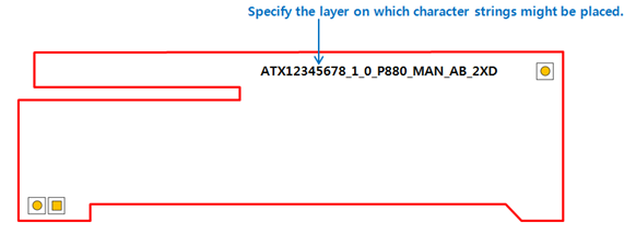
Layer Selection: Define the layer from the artwork layer list, then
use PollEx DFM to verify that it contains
character string data.
Delimiter: Divide string into several parts. In the example below,
if the delimiter is, _ , there may be seven parts.
Ignore String-Index from Back: From the back end, If there
is an identical amount of items as the given integer number,
it is meaningless. If the integer assigned is two for this
value, six and seven will become meaningless. From this
point, PollEx DFM handles the
strings, ATX12345678_1_0_P880_MAN. This is the same as
trimming to the right as many as the specified number using
the delimiter.
Exclude Character: If newly generated character strings have
unnecessary characters, enter them here. For example, if a character
string has }, delete it in the string and enter it into the
column.
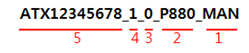
Revision Index from Back: Define the revision number string index
from the back. If the output character string is
ATX12345678_1_0_P880_MAN and won’t get revision number 1, use an
integer. Figure 6.
This means the fourth index from the back is 1 and it is the
revision number.
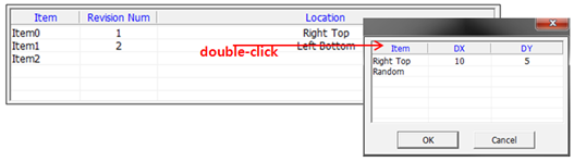
Revision Index Table: Use this table to define the fiducial mark
location depending on the revision number. Figure 7.
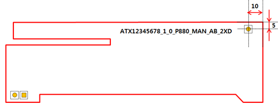
If the revision number is 1 in the table, the fiducial mark
should be on location 10 and 5 apart from the top right corner of
the board. Figure 8.
Remainder: Set all the unspecified revision number locations.